UCLA Electrical Engineers Develop Energy-Efficient and Customizable Chip Design to Maximize Data Processing
Energy-efficient and customizable chip design by UCLA researchers to maximize data processing
Now, UCLA electrical engineers have designed a new type of computer chip that takes advantage of the increasingly underutilized processing areas.
The problem of inefficiency in dark silicon areas has cropped up over the past decade. While transistors have continued to get smaller, the chip’s power consumption has remained the same, leading to power shortages if all the transistors are in use simultaneously. To stay within the power limit, only transistors in certain areas are “turned on” at any one time. However, the in-use areas are usually occupied by energy-efficient yet inflexible hardware accelerator blocks designed to execute a growing number of hard-coded functions.
Led by Dejan Markovic, professor of electrical and computer engineering at the UCLA Samueli School of Engineering, the team has introduced a new energy-efficient chip design that maximizes the areas set aside for data-intensive processing while minimizing areas of dark silicon. Earlier this year, the UCLA researchers presented their study at the 2022 International Solid-States Circuits Conference. Theirs was the only paper authored by a group of university researchers, with industry representatives giving the rest of the presentations.
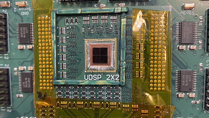
“The key to our chip design is its network of multiple connecting layers over the core processing elements. This minimizes delays and maximizes the total area being used,” Dejan Markovic said.
“The key to our chip design is its network of multiple connecting layers over the core processing elements. This minimizes delays and maximizes the total area being used,” Markovic said. “Like a network of in-sync traffic lights, the smart network moves and manages data processing and computing applications efficiently across the entire network of billions of transistors.”
According to the researchers, their network’s operation is driven by real-time usage statistics along with a switch box that controls which parts of the processing elements are in use, thereby maximizing energy efficiency. The design is also reconfigurable, so it can be tailored for specific applications.
Titled “A 16nm 785GMACs/J 784-Core Digital Signal Processor Array with a Multilayer Switch Box Interconnect, Assembled as a 2×2 Dielet with 10μm-Pitch Inter-Dielet I/O for RuntimeMulti-Program Reconfiguration,” the paper is accessible at the IEEE Xplore Library.
Other authors are UCLA graduate students Uneeb Rathore and Sumeet Singh Nagi, as well as Subramanian Iyer, distinguished professor of electrical and computer engineering at UCLA Samueli and holder of the Charles P. Reames Endowed Chair in Electrical Engineering.