With residential energy costs at just over 11 cents per kilowatt hour, according to the latest figures from the U.S. Energy Information Administration, the savings are significant and growing, so far totaling well over $100 million that consumers haven’t been charged on their electricity bills.
Electronics are constantly leaking power, and that energy is wasted without having contributed anything to performance. This is especially true of devices that consumers tend to leave turned on even when they aren’t being used, such as personal computers, cell phones, and cable and Internet connections.
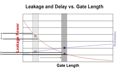
The technology, co-invented in 2003 by UC San Diego Jacobs School of Engineering Professor Andrew B. Kahng and Puneet Gupta, now an assistant professor of electrical engineering at the UCLA Henry Samueli School of Engineering and Applied Science Professor, subtly modifies the dimensions of transistors, the tiny switches that control the flow of electricity in an integrated circuit. This approach, known as “gate-length biasing,” exploits the fact that slower transistors leak less power. The invention essentially ensures that transistors on a chip are as slow as possible without affecting performance.
The technology is now widely used in numerous applications such as network processors, Internet routers and the graphics processing units (GPUs) that are found in personal computers, tablets and game consoles.
UC San Diego first licensed the then-patent-pending invention in 2004 to a startup company, Blaze DFM, which Kahng and Gupta, then a student of Kahng’s, co-founded. The patent was subsequently awarded in 2006 to UC San Diego and the University of Michigan. Gupta returned to the Jacobs School in 2007 to finish his Ph.D. Blaze DFM was acquired by Tela Innovations in 2009.
Kahng and Gupta solved a complex optimization problem to identify which transistors can be slowed down. And they had to do this without changing the way chip designs are handed off from design teams to the silicon foundries that manufacture the chips.
“As transistor dimensions continue to shrink in advanced manufacturing technologies, the potential for wasted energy only increases,” said Gupta. “By adding even a few nanometers to the channel length of a transistor – using gate-length biasing – the invention substantially reduces leakage power while only slightly slowing down the transistor’s switching speed.”
“The key is figuring out which of the hundreds of millions of transistors on the chip to modify,” added Kahng. “Many, but not all, of the transistors can be made slower without affecting the clock frequency. We developed a tool to maximize leakage power savings without affecting product performance, and we created a flow to make this transparent and easy for both designers and manufacturers.”
As the technology is more widely deployed, the energy and cost savings continue to accelerate.
“Since the Blaze MO product was launched in 2006, energy consumption reductions – in products ranging from GPUs to mobile communication integrated circuits – achieved by our licensees using Tela’s patented Gate Length Biasing technology have conservatively amounted to over 1 trillion watt-hours,” said Rajiv Bhateja, Vice President of Power Optimization Products at Tela Innovations.
The gate-length biasing approach exemplifies the increasingly close coupling between design and manufacturing that is needed to keep Moore’s Law on track in today’s advanced technologies.
Gupta and his UCLA research group are widely recognized for pioneering work at the semiconductor design-manufacturing interface, resulting in reduced costs and improved efficiency of silicon chips.
“Power has long been one of the key constraints for advanced chips, especially for mobile applications,” said Riko Radojcic, director at Qualcomm CDMA Technologies. “Qualcomm has been one of the early evaluation partners with Blaze technology, and demonstrated the leakage power reductions achieved by the Blaze optimization tool and gate-length biasing methodology on a baseband processor chip, starting at the 90nm technology node. It is gratifying to see such success for a technology that originated just a few miles away on the UC San Diego campus. I always look forward to the next ideas from Professors Kahng and Gupta.”
Main Image: Smart gate-length biasing: optimization decides the bias to use for each one of billions of transistors; manufacturing tools implement the biases transparently.