UCLA researchers have a plan to redesign computer chips from the ground up to make smaller, cheaper, and more dynamic electronic devices.
If you crack open any of the electronic devices you use on a daily basis— your phone, smartwatch, tablet, TV, instant pot or microwave— you’ll see a landscape reminiscent of a miniscule city map. Computer chips, each dotted with microscopic transistors, are arranged like buildings on the green grid of a circuit board. The view you see is roughly how the insides of computers have looked for the past half century. But UCLA researchers at the Center for Heterogeneous Integration and Performance Scaling (CHIPS) say that computers powered on these chips are reaching their limits and a redesign is needed. Their work aims to make the innards of electronics fundamentally different, and will, in turn, allow new generations of flexible, implantable, faster, cheaper, smaller and more powerful systems, they say.
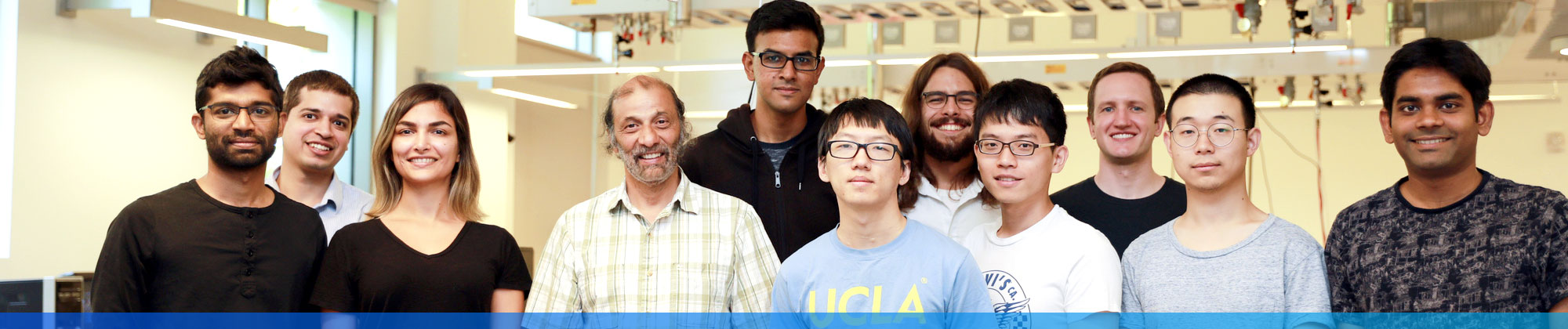
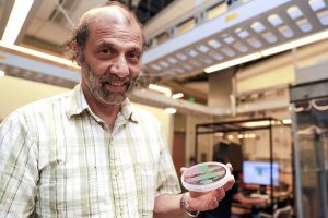 “It will make possible things that weren’t possible before,” said Subramanian Iyer, a UCLA professor of electrical and computer engineering, and director of CHIPS.
Every two years since 1965, the number of transistors on a computer chip has roughly doubled, as transistors have gotten exponentially smaller. In practical terms, this doubling—dubbed Moore’s Law— has meant faster, smaller, cheaper and more powerful computers. But as transistors reach the tiniest atomic size allowed by material properties and physics, this doubling is due to stall.
“We can’t keep making transistors smaller in an economical way,” said Iyer, who, before joining the UCLA faculty, worked for 30 years at IBM, where he helped design, develop and manufacture new semiconductor technologies. “We have to look at other ways of scaling the technology.”
Shrinking the Circuit Board
As computer chips have gotten more powerful, crammed with now billions of transistors, the layout of chips on a circuit board hasn’t changed much. Each chip—also called an integrated circuit—is spaced relatively far apart from its neighbors, with long, visible wires connecting them. The organization is large and slows things down.
“The energy it takes to communicate between chips has not changed; if anything, it has gone up,” Iyer said. It’s a bit like having old, outdated roads trying to support a growing, bustling city, he says.
At CHIPS, Iyer and his colleagues are replacing run-of-the-mill circuit boards with silicon wafers. Since transistors themselves are made of silicon, the researchers can precisely align individual integrated circuits of transistors, called dies, onto each wafer. This allows all these dies to act as if they were one giant chip the size of the wafer, which can be as large as 70,000 square millimeters, which is about the same area as a large dinner plate. In contrast the largest chips made today are about 100-times smaller, or around 700 square millimeters.
Today’s single large chips, called SoCs for system-on-a-chip, are expensive to make and use dies that must be manufactured at the same time in the same process. For example, if you need both memory and processors you would have to compromise the performance of one, the other or both to make them in a single process.
The platforms being developed at UCLA can use dies from a variety of sources that can me mixed and matched.
“In separate processes, we can make memory and processor dies and not make any sacrifices in performance for either component,” Iyer said. “This heterogeneity is another unique capability of our platforms.”
Moreover, the dies be packed together far more closely than bulky chips and the silicon wires that connect them can be mere nanometers wide. A square of Silicon Interconnect Fabric (Si-IF), as they’ve named it, is many times smaller than a corresponding printed circuit board with the same capabilities.
“The closeness of things makes an advantage in performance in terms of energy and time it takes to do things,” said Boris Vaisband, a postdoctoral researcher at CHIPS who has worked on the project.
Si-IF has other advantages to printed circuit boards as well; it weighs less, larger networks can be assembled in a smaller space, and, using a technology the team is calling Flextrate, it can be made to be completely flexible. These properties, the researchers say, make Si-IF, and Flextrate, especially ideal for medical devices. They’re collaborating with physicians and biomedical engineers to develop applications of the technology.
“It’s difficult to predict all the ways this will be used,” Iyer said. “We make the platform and then innovators hopefully take it from there.”
At Cal State Los Angeles, physiology and neuroscience researcher Selvan Joseph is one such innovator. He’s using the Flextrate platform developed at CHIPS to design sensors that can track the physical movements and muscle activity of patients with movement disorders, or those recovering from spinal cord injuries. Flextrate allows him to put these sensors in a small flexible patch that patients can wear unobtrusively on their skin.
“This technology is definitely a game-changer in that you can create devices with more flexibility, pliability and portability,” Joseph said. “We can send this device home with our patients and then remote collect data in real time in their day-to-day lives.”

Faster Communication
While these platforms have the potential to revolutionize data centers, and consumer and medical electronics, the CHIPS team is also working on ways to make supercomputers and artificial intelligence machines more powerful in the wake of Moore’s Law.
Today, tools called inference engines are behind most of the “smart” electronics in our daily lives. An inference engine collects data and makes logical conclusions. Search engines, virtual assistants like Apple’s Siri or Amazon’s Alexa, and self-driving cars all rely on inference engines. But the speed of these is limited by the fact that, to make an inference, the device must relay information back and forth between the memory and processing centers of a device.
Iyer and his colleagues at CHIPS have invented a charge trap transistor (CTT) which combines the memory and processing centers such that this constant back-and-forth is no longer needed. It saves both time and energy, Iyer said.
“We can make inferences in a CTT 100 times more efficiently than the most efficient inference engine out there,” he said. “We’ve demonstrated this on a small scale and are starting to add on more bells and whistles now.”
Shrinking transistors have driven the technology leaps of the last fifty years, but Iyer says those days are over. The question is, how will technology continue to improve without improvements in transistors? Making the leap to new kinds of devices, such as those that use Si-IF and CTTs, is one feasible answer but requires a buy-in from technology companies. That’s in part why CHIPS has organized a consortium with industry leaders to validate and shape the direction of the center.
“The problem isn’t technical right now,” Iyer said. “It’s psychological. The industry has to turn on a dime and embrace this new way of doing things which is a complete break from how they’ve been doing things.”