The UCLA Department of Materials Science and Engineering has obtained a dual-beam focused ion beam (FIB) – scanning electron microscope (SEM) system – a very advanced 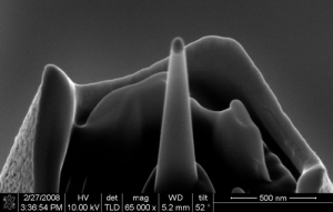 imaging and nanomanufacturing instrument that can create, modify, and image complex structures that are a few tens of nanometers in size.
A focused ion beam (FIB) system uses ions – positively charged atoms – to create three-dimensional structures through the removal (or addition) of material in a precise and highly controlled manner down to nanometer scales. Much like carving in stone, this system allows users to manipulate and/or fabricate complex shapes and sizes.
This system equipped with a SEM, which uses electrons to “see” surfaces of materials with nanometer resolution, enables visualization of as-fabricated structures.
“This newly acquired instrument will allow researchers, both here at UCLA and outside, 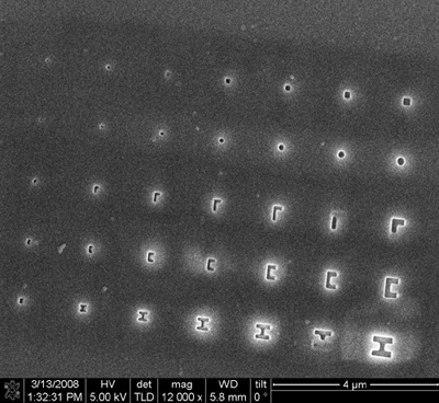 to create new complex nanostructures of a wide variety of materials,” said Suneel Kodambaka, assistant professor of materials science and engineering. “Here at the Department of Materials Science and Engineering, we are very excited about the prospects of using this instrument for several advanced research projects. Researchers in academia and in industry have already found the FIB-SEM to be a valuable tool for their work and we are pleased that it is available as a user facility.” Sergey Prikhodko, staff scientist in Materials Science and Engineering, is in-charge of the operation and maintenance of the dual-beam SEM/FIB system, which will be under the supervision of Steve Franz, manager of the Nanoelectronics Research Facility.
* See the Nanolab’s website for details: http://www.nanolab.ucla.edu/
* To view a step-by-step transmission electron microscope sample preparation of a carbon fiber reinforced Zr-ZrC matrix composite, using the FIB-SEM, click here.
From materials science and engineering professor Jenn-Minn Yang’s research group. Preparation by Noah Bodzin of the UCLA Department of Physics and Sergey Prikhodko of Materials Science and Engineering.
Main Image: The scale bar on both images is 1 µm. The use of ions allows a FIB system to create three-dimensional structures through the removal of material by sputtering in a precise and highly controlled manner down to nanometer scales. Much like carving in stone, this system allows users to determine shapes and depth of their cuts. Figures 1 and 2 shows structures fabricated using a Nova 600 on Si wafer by Noah Bodzin. The size of the pitch on Figure 2 is 50 nm.
Inset Images: The research group of Sakhrat Khizroev, assistant professor of electrical engineering at UC Riverside, used FIB for rapid prototyping of nanomagnetic devices to enable next-generation information storage and logic technologies as well as medicine and energy harvesting related applications. Figure 3 shows a FIB fabricated magnetic force microscopy (MFM) tip in the form of a point dipole deposited on the tip of a silicon etched probe.
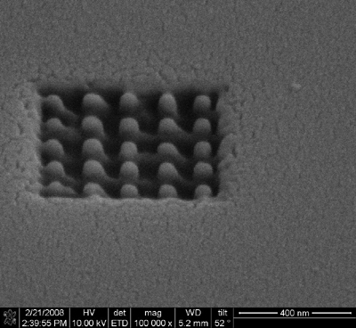
Figure 4 shows nanoscale apertures fabricated using Nova 600 at UCLA by Andrey Lavrenov for the on-going study of heat-assisting magnetic recording (HAMR) suitable for areal densities above 10 terabit/In2. The set of apertures is milled into a 150 nm thick aluminum film sputtered on the emitting edge of a semiconducting diode. Figure 5 shows FIB-fabricated patterned media with a bit side of 50 nm milled into 50-nm thick magnetic media.